STM32F103 Mini
Overview
The STM32F103_MINI board features an ARM Cortex-M3 based STM32F103RC MCU
with a wide range of connectivity support and configurations. There are
multiple version of this board like stm32f103_mini.
Hardware
STM32F103 Mini provides the following hardware components:
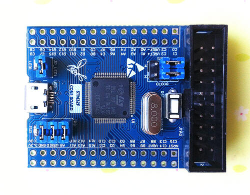
STM32 microcontroller in QFP64 package
Flexible board power supply:
USB VBUS or external source (3.3V, 5V, 7 - 12V)
Power management access point
Two LEDs:
User LED (LD1), power LED (LD2)
USB re-enumeration capability:
Mass storage
More information about STM32F103RC can be found here:
Supported Features
The stm32f103_mini board supports the hardware features listed below.
- on-chip / on-board
- Feature integrated in the SoC / present on the board.
- 2 / 2
-
Number of instances that are enabled / disabled.
Click on the label to see the first instance of this feature in the board/SoC DTS files. -
vnd,foo -
Compatible string for the Devicetree binding matching the feature.
Click on the link to view the binding documentation.
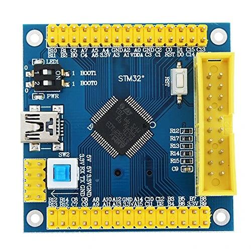
Connections and IOs
Each of the GPIO pins can be configured by software as output (push-pull or open-drain), as input (with or without pull-up or pull-down), or as peripheral alternate function. Most of the GPIO pins are shared with digital or analog alternate functions. All GPIOs are high current capable except for analog inputs.
Board connectors:
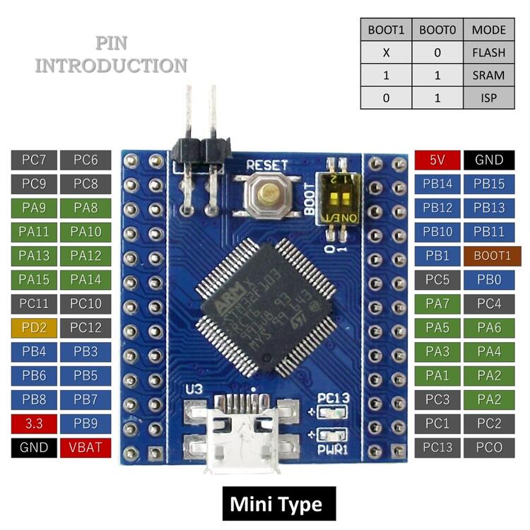
Default Zephyr Peripheral Mapping:
UART_1 TX/RX: PA9/PA10
UART_2 TX/RX: PA2/PA3 (ST-Link Virtual COM Port)
SPI1 NSS/SCK/MISO/MOSI: PA4/PA5/PA6/PA7
SPI2 NSS/SCK/MISO/MOSI: PB12/PB13/PB14/PB15
I2C1 SDA/SCL: PB9/PB8
PWM1_CH1: PA8
USER_PB: PC13
LD1: PA5
USB_DC DM/DP: PA11/PA12
System Clock
The on-board 8MHz crystal is used to produce a 72MHz system clock with PLL.
Programming and Debugging
The stm32f103_mini board supports the runners and associated west commands listed below.
| flash | debug |
|---|
Applications for the stm32f103_mini board configuration can be built and
flashed in the usual way (see Building an Application and
Run an Application for more details).
Flashing
There are 2 main entry points for flashing STM32F1X SoCs, one using the ROM bootloader, and another by using the SWD debug port (which requires additional hardware such as ST-Link). Flashing using the ROM bootloader requires a special activation pattern, which can be triggered by using the BOOT0 pin.
Flashing an application to stm32f103 mini
Here is an example for the Blinky application.
# From the root of the zephyr repository
west build -b stm32f103_mini samples/basic/blinky
west flash
You will see the LED blinking every second.
Debugging
You can debug an application in the usual way. Here is an example for the Blinky application.
# From the root of the zephyr repository
west build -b stm32f103_mini samples/basic/blinky
west debug