RA4W1 Evaluation Kit
Overview
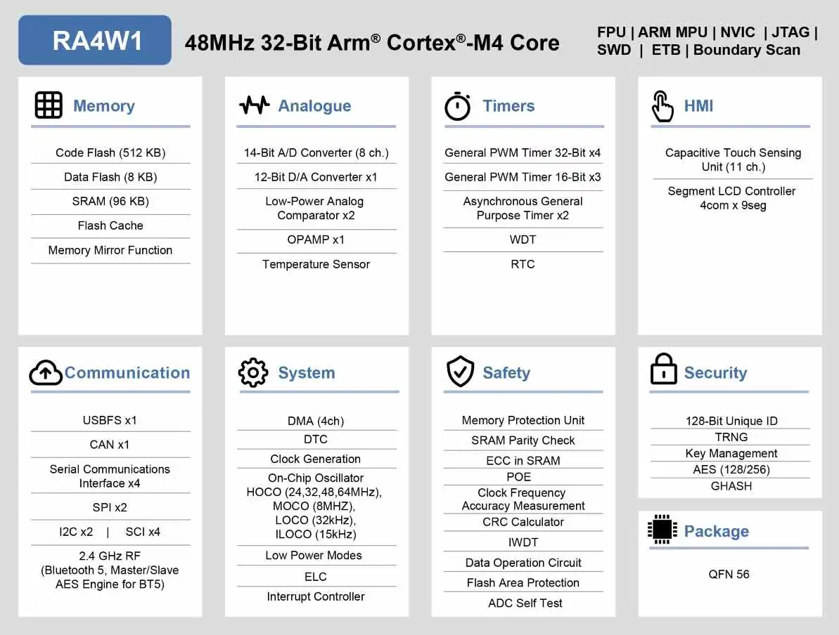
The Renesas RA4W1 is the first Bluetooth® 5.0 Low Energy fully compliant with 2Mbit High-Throughput (HT) and Long Range support in a single chip MCU of Renesas RA4 product series for IoT applications that require a high-performance Arm® Cortex®-M4 core at a very attractive price point. The RA4W1 MCU has full function support for Bluetooth 5.0 Low Energy long-range and mesh networking, and provides excellent reception performance. RA4W1 is geared towards IoT application requiring Security, large embedded RAM and low power consumption.
MCU Native Pin Access
R7FA4W1AD2CNG
QFN-56 package
On-chip memory: 512-KB ROM, 96-KB RAM, 8-KB data flash memory
Power-supply voltage
USB connector: 5-V input
Power-supply IC: 5-V input, 3.3-V output
External power-supply header*1: 3.3-V input, 2 pins x 1
Main clock
Crystal oscillator (surface-mount technology (SMT)) for the main system clock
Crystal oscillator or ceramic resonator (lead type) for the main system clock
Sub-clock
Crystal oscillator (SMT) for the sub-clock
Bluetooth Low Energy
Bluetooth Low Energy (BLE) circuit x1
Range of frequency: 2402 to 2480 MHz
Maximum transmission output power: 4 dBm (in 4-dBm output mode)
Output variation: +2 dB
Push switches
Reset switch x 1
User switch x 1
LED
Power indicator: green x 1
User: green x 2
ACT LED: green x 1
Connectivity
Connector for an on-board emulator: USB Micro-B
Connector for a USB serial-conversion interface: USB Micro-B
Pmod™ connector: Angle type, 12 pins
Arduino™ UNO connectors
Emulator reset switch: DIP switch x 1
Hardware
Detailed Hardware features for the RA4W1 MCU group can be found at RA4W1 Group User’s Manual Hardware
RA4W1 Block diagram (Credit: Renesas Electronics Corporation)
Detailed Hardware features for the EK-RA4W1 MCU can be found at EK-RA4W1 - User’s Manual
Supported Features
The ek_ra4w1 board supports the hardware features listed below.
- on-chip / on-board
- Feature integrated in the SoC / present on the board.
- 2 / 2
-
Number of instances that are enabled / disabled.
Click on the label to see the first instance of this feature in the board/SoC DTS files. -
vnd,foo -
Compatible string for the Devicetree binding matching the feature.
Click on the link to view the binding documentation.
Programming and Debugging
The ek_ra4w1 board supports the runners and associated west commands listed below.
| flash | debug |
|---|
Applications for the ek_ra4w1 board target configuration can be
built, flashed, and debugged in the usual way. See
Building an Application and Run an Application for more details on
building and running.
Flashing
Program can be flashed to EK-RA4W1 via the on-board SEGGER J-Link debugger. SEGGER J-link’s drivers are available at https://www.segger.com/downloads/jlink/
To flash the program to board
Connect to J-Link OB via USB port to host PC
Make sure J-Link OB jumper is in default configuration as describe in EK-RA4W1 - User’s Manual
Execute west command
west flash -r jlink
Debugging
You can use Segger Ozone (Segger Ozone Download) for a visual debug interface
Once downloaded and installed, open Segger Ozone and configure the debug project like so:
Target Device: R7FA4W1AD
Target Interface: SWD
Target Interface Speed: 4 MHz
Host Interface: USB
Program File: <path/to/your/build/zephyr.elf>
Note: It’s verified that we can debug OK on Segger Ozone v3.30d so please use this or later version of Segger Ozone